In recent years semiconducting organic-inorganic lead halide perovskite materials have gained much interest due to their outstanding optoelectronic properties for use in solar cells and lighting applications. A major drawback of these materials is related to their toxicity and chemical instability. Recently, purely inorganic transition metal perovskite chalcogenides (TMPC) have been synthesized that exhibit promising (opto-)electronic properties and may even allow opto- electrochemical applications. Compared to their perovskite oxide counterparts of type ABO3 (A = alkali, alkaline, or rare earth metal, B = transition metal) with a large electronic bandgap (EG > 3eV), many perovskite chalcogenides exhibit an electronic bandgap in visible light spectrum that is related to the replacement of O by S or Se in the crystal lattice and which may enable a broad spectrum of applications. In this work, the piezoelectric properties of the new compound semiconductor material stand in the foreground.
Entering now into the third phase, this project aims to grow crystalline (single ~ and poly ~) BaZrS3 layers as already developed in the first and second project phase and apply them in electronic test devices for regenerative energy harvesting. For this purpose, the piezo and potentially ferroelectric material properties will be studied using fundamental materials characterization tools as well as application related test environments. The final goal is to build a simple demonstrator which converts mechanical into electrical energy.
Principal Investigators
 | Prof. Dr. Peter Wellmann Institute of Materials for Electronics and Energy Technology Department of Materials Science and Engineering Friedrich-Alexander-Universität Erlangen peter.wellmann@fau.de |
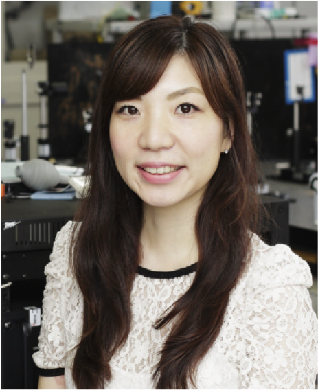
 | Prof. Dr. Reina Miyagawa Physical Science and Engineering Department Nagoya Institute of Technology, Japan miyagawa.reina@nitech.ac.jp |
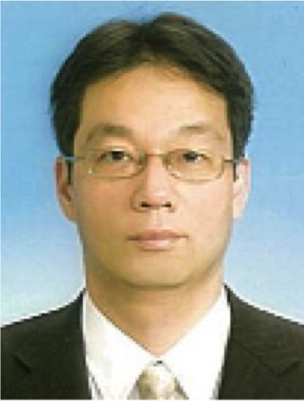
 | Prof. Dr. Masashi Kato Department of Electrical and Mechanical Engineering Nagoya Institute of Technology, Japan kato.masashi@nitech.ac.jp |
 | Prof. Dr. Koichi Hayashi Physical Science and Engineering Department Frontier Research Institute for Materials Science Nagoya Institute of Technology, Japan hayashi.koichi@nitech.ac.jp |
 | Prof. Dr. Koji Kimura Physical Science and Engineering Department Frontier Research Institute for Materials Science Nagoya Institute of Technology, Japan kimura.koji@nitech.ac.jp |
Doctoral Researchers
 | Arya Raghunadhan Nair, M. Sc. Institute of Materials for Electronics and Energy Technology Department of Materials Science and Engineering Friedrich-Alexander-Universität Erlangen arya.r.nair@fau.de |
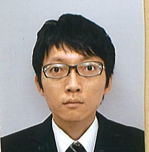
 | Kongshik Rho, M. Sc. Electrical and Mechanical Engineering Department Frontier Research Institute for Materials Science Nagoya Institute of Technology, Japan k.rho.991@stn.nitech.ac.jp |
